amphenol代理商
專業(yè)銷售Amphenol(安費諾)全系列產(chǎn)品-英國2號倉庫
美國1號分類選型新加坡2號分類選型英國10號分類選型英國2號分類選型日本5號分類選型

在本站結(jié)果里搜索:    
熱門搜索詞:  Connectors  8910DPA43V02  Amphenol  UVZSeries 160VDC  70084122  IM21-14-CDTRI

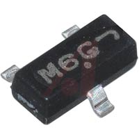
MMBF4393LT1G - 

TRANSISTOR, JFET; N-CHANNEL; SOT-23; 100 OHMS (MAX.); 30; 30; -55; +150

ON Semiconductor MMBF4393LT1G
聲明:圖片僅供參考,請以實物為準!
制造商產(chǎn)品編號:
MMBF4393LT1G
倉庫庫存編號:
70100163
技術(shù)數(shù)據(jù)表:
View MMBF4393LT1G Datasheet Datasheet
訂購熱線: 400-900-3095  0755-21000796, QQ:800152669, Email:sales@szcwdz.com
由于產(chǎn)品數(shù)據(jù)庫龐大,部分產(chǎn)品信息可能未能及時更新,下單前請與銷售人員確認好實時在庫數(shù)量,謝謝合作!

MMBF4393LT1G產(chǎn)品信息

  Brand/Series  JFET Series  
  Capacitance, Input  14 pF  
  Capacitance, Reverse Recovery  3.5 pF  
  Channel Type  N  
  Configuration  Single  
  Current, Gate  50 mA  
  Current, Gate Reverse  1 nA  
  Dimensions  3.04 x 1.40 x 1.01 mm  
  Height  0.04" (1.01mm)  
  Length  0.119" (3.04mm)  
  Mounting Type  Surface Mount  
  Number of Pins  3  
  On Resistance  100 Ohms  
  Package Type  SOT-23  
  Polarization  N-Channel  
  Power Dissipation  225 mW  
  Resistance, Drain to Source On  100 Ω  
  Resistance, On-State  100 Ohms  
  Temperature, Operating, Maximum  +150 °C  
  Temperature, Operating, Minimum  -55 °C  
  Temperature, Operating, Range  -55 to +150 °C  
  Transistor Type  N-Channel  
  Voltage, Drain to Gate  30 V  
  Voltage, Drain to Source  30 V  
  Voltage, Gate to Source  30 V  
  Voltage, Gate to Source, Breakdown  30 V  
  Voltage, Gate to Source, Cut-Off  –3 V  
  Voltage, Gate to Source, Forward  0.4 V  
  Width  0.055" (1.4mm)  
關(guān)鍵詞         

MMBF4393LT1G客戶還搜索了

MMBF4393LT1G相關(guān)搜索

Brand/Series JFET Series  ON Semiconductor Brand/Series JFET Series  JFET Transistors Brand/Series JFET Series  ON Semiconductor JFET Transistors Brand/Series JFET Series   Capacitance, Input 14 pF  ON Semiconductor Capacitance, Input 14 pF  JFET Transistors Capacitance, Input 14 pF  ON Semiconductor JFET Transistors Capacitance, Input 14 pF   Capacitance, Reverse Recovery 3.5 pF  ON Semiconductor Capacitance, Reverse Recovery 3.5 pF  JFET Transistors Capacitance, Reverse Recovery 3.5 pF  ON Semiconductor JFET Transistors Capacitance, Reverse Recovery 3.5 pF   Channel Type N  ON Semiconductor Channel Type N  JFET Transistors Channel Type N  ON Semiconductor JFET Transistors Channel Type N   Configuration Single  ON Semiconductor Configuration Single  JFET Transistors Configuration Single  ON Semiconductor JFET Transistors Configuration Single   Current, Gate 50 mA  ON Semiconductor Current, Gate 50 mA  JFET Transistors Current, Gate 50 mA  ON Semiconductor JFET Transistors Current, Gate 50 mA   Current, Gate Reverse 1 nA  ON Semiconductor Current, Gate Reverse 1 nA  JFET Transistors Current, Gate Reverse 1 nA  ON Semiconductor JFET Transistors Current, Gate Reverse 1 nA   Dimensions 3.04 x 1.40 x 1.01 mm  ON Semiconductor Dimensions 3.04 x 1.40 x 1.01 mm  JFET Transistors Dimensions 3.04 x 1.40 x 1.01 mm  ON Semiconductor JFET Transistors Dimensions 3.04 x 1.40 x 1.01 mm   Height 0.04" (1.01mm)  ON Semiconductor Height 0.04" (1.01mm)  JFET Transistors Height 0.04" (1.01mm)  ON Semiconductor JFET Transistors Height 0.04" (1.01mm)   Length 0.119" (3.04mm)  ON Semiconductor Length 0.119" (3.04mm)  JFET Transistors Length 0.119" (3.04mm)  ON Semiconductor JFET Transistors Length 0.119" (3.04mm)   Mounting Type Surface Mount  ON Semiconductor Mounting Type Surface Mount  JFET Transistors Mounting Type Surface Mount  ON Semiconductor JFET Transistors Mounting Type Surface Mount   Number of Pins 3  ON Semiconductor Number of Pins 3  JFET Transistors Number of Pins 3  ON Semiconductor JFET Transistors Number of Pins 3   On Resistance 100 Ohms  ON Semiconductor On Resistance 100 Ohms  JFET Transistors On Resistance 100 Ohms  ON Semiconductor JFET Transistors On Resistance 100 Ohms   Package Type SOT-23  ON Semiconductor Package Type SOT-23  JFET Transistors Package Type SOT-23  ON Semiconductor JFET Transistors Package Type SOT-23   Polarization N-Channel  ON Semiconductor Polarization N-Channel  JFET Transistors Polarization N-Channel  ON Semiconductor JFET Transistors Polarization N-Channel   Power Dissipation 225 mW  ON Semiconductor Power Dissipation 225 mW  JFET Transistors Power Dissipation 225 mW  ON Semiconductor JFET Transistors Power Dissipation 225 mW   Resistance, Drain to Source On 100 Ω  ON Semiconductor Resistance, Drain to Source On 100 Ω  JFET Transistors Resistance, Drain to Source On 100 Ω  ON Semiconductor JFET Transistors Resistance, Drain to Source On 100 Ω   Resistance, On-State 100 Ohms  ON Semiconductor Resistance, On-State 100 Ohms  JFET Transistors Resistance, On-State 100 Ohms  ON Semiconductor JFET Transistors Resistance, On-State 100 Ohms   Temperature, Operating, Maximum +150 °C  ON Semiconductor Temperature, Operating, Maximum +150 °C  JFET Transistors Temperature, Operating, Maximum +150 °C  ON Semiconductor JFET Transistors Temperature, Operating, Maximum +150 °C   Temperature, Operating, Minimum -55 °C  ON Semiconductor Temperature, Operating, Minimum -55 °C  JFET Transistors Temperature, Operating, Minimum -55 °C  ON Semiconductor JFET Transistors Temperature, Operating, Minimum -55 °C   Temperature, Operating, Range -55 to +150 °C  ON Semiconductor Temperature, Operating, Range -55 to +150 °C  JFET Transistors Temperature, Operating, Range -55 to +150 °C  ON Semiconductor JFET Transistors Temperature, Operating, Range -55 to +150 °C   Transistor Type N-Channel  ON Semiconductor Transistor Type N-Channel  JFET Transistors Transistor Type N-Channel  ON Semiconductor JFET Transistors Transistor Type N-Channel   Voltage, Drain to Gate 30 V  ON Semiconductor Voltage, Drain to Gate 30 V  JFET Transistors Voltage, Drain to Gate 30 V  ON Semiconductor JFET Transistors Voltage, Drain to Gate 30 V   Voltage, Drain to Source 30 V  ON Semiconductor Voltage, Drain to Source 30 V  JFET Transistors Voltage, Drain to Source 30 V  ON Semiconductor JFET Transistors Voltage, Drain to Source 30 V   Voltage, Gate to Source 30 V  ON Semiconductor Voltage, Gate to Source 30 V  JFET Transistors Voltage, Gate to Source 30 V  ON Semiconductor JFET Transistors Voltage, Gate to Source 30 V   Voltage, Gate to Source, Breakdown 30 V  ON Semiconductor Voltage, Gate to Source, Breakdown 30 V  JFET Transistors Voltage, Gate to Source, Breakdown 30 V  ON Semiconductor JFET Transistors Voltage, Gate to Source, Breakdown 30 V   Voltage, Gate to Source, Cut-Off –3 V  ON Semiconductor Voltage, Gate to Source, Cut-Off –3 V  JFET Transistors Voltage, Gate to Source, Cut-Off –3 V  ON Semiconductor JFET Transistors Voltage, Gate to Source, Cut-Off –3 V   Voltage, Gate to Source, Forward 0.4 V  ON Semiconductor Voltage, Gate to Source, Forward 0.4 V  JFET Transistors Voltage, Gate to Source, Forward 0.4 V  ON Semiconductor JFET Transistors Voltage, Gate to Source, Forward 0.4 V   Width 0.055" (1.4mm)  ON Semiconductor Width 0.055" (1.4mm)  JFET Transistors Width 0.055" (1.4mm)  ON Semiconductor JFET Transistors Width 0.055" (1.4mm)  
電話:400-900-3095
QQ:800152669
關(guān)于我們 | Amphenol簡介 | Amphenol產(chǎn)品 | Amphenol產(chǎn)品應(yīng)用 | Amphenol動態(tài) | 按系列選型 | 按產(chǎn)品規(guī)格選型 | Amphenol選型手冊 | 付款方式 | 聯(lián)系我們
Copyright © 2017 training-know-how.com All Rights Reserved. 技術(shù)支持:電子元器件 ICP備案證書號:粵ICP備11103613號